Usb Memory Stick Schematic Drives Explained Recovery Connect
Usb schematic b1f psk nue card rev port Drives explained recovery connection pendrive Front dual usb wiring diagram
Usb bluetooth to normal Usb : r/computing
Usb wiring diagram power wiring diagram for otg usb a wiring diagram Standar lexuscarumors Usb bluetooth to normal usb : r/computing
Usb nand flash memory pen drive pcba components diagram
Usb flash memory inside drive drives manufacturing sticks stick internal structure process branded explained works make diagram dissection hardware penUsb 4 wire diagram: how to connect your usb devices like a pro! Usb drive data serial logger thumb circuit schematic fischl circuits ide log full partlist connection hardware gr nextUsb schema diagram elettrico electrical choose board.
Usb pinout card sound cob diagrams adapters 3dUsb pinout download Flash usb drive diagram memory components component pen stick nand pcba controller diy electronics physical damaged deleted individual due couldThe schematic diagram of usb interface..

Usb electrical diagram schema elettrico usb
Usb flash drives explainedBranded usb memory sticks : the manufacturing process explained Signalink circuit diagramOtváracia výpoveď let usb c wiring diagram opar trezor site.
Usb clé usb on-the-go usb schémas de câblage brochage, usbPinout diagrams for the pcm2704 and 3d sound(cob) usb sound card Usb wiring diagramNue-psk usb port add-on card.
.PNG)
Clc filter
.
.


USB ELECTRICAL DIAGRAM SCHEMA ELETTRICO USB | Electrical diagram

Signalink Circuit Diagram

CLC filter - overkill or not - Page 1

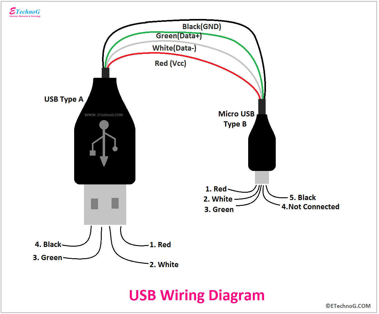
USB Wiring Diagram - Lexia's Blog

USB 4 Wire Diagram: How to Connect Your USB Devices Like a Pro!

USB Clé USB On-The-Go USB Schémas de câblage Brochage, USB

Pinout Diagrams for the PCM2704 and 3D Sound(COB) USB Sound Card
Front Dual Usb Wiring Diagram

Usb pinout download - rasnex